Seeing that CNC milling of PCBs is a hot topic right now, i figured i should make a post of what learning I have had from doing it, and getting workable results using an MPCNC.
This post is as much documentation for me for next time I have to do this, as it is for everyone else.
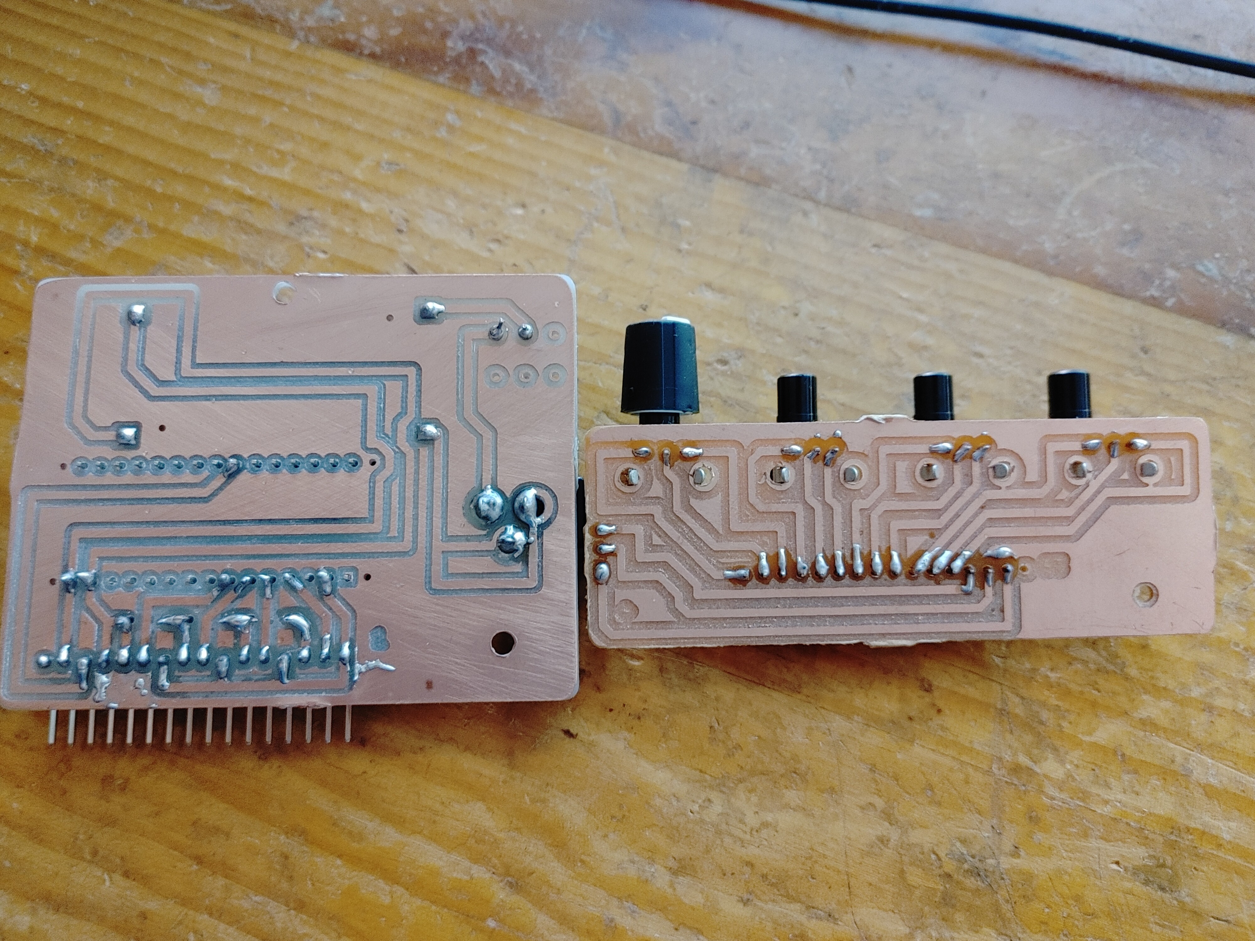
Firstly the results (ignore my horrible soldering job please)
Learnings section.
-
level is king
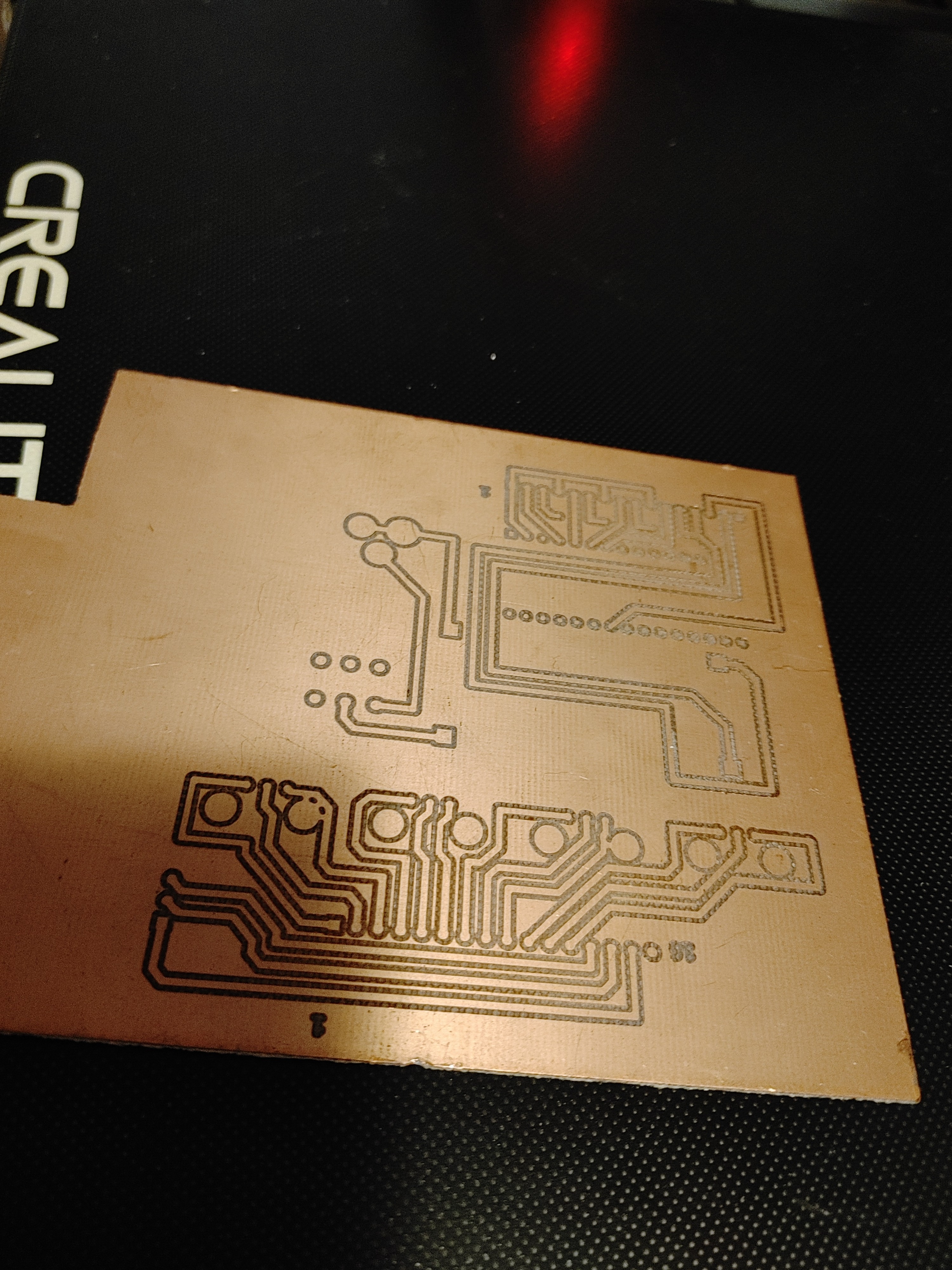
I was using 0.2mm 30deg V bits to do the isolation milling. These are really sensitive to not being absolutely flat, because the cut depth (and hence width) rapidly changes with even small variations in Z.
I used bCNC’s autolevel function and a probe to to convert the gcode on the fly, but there is other ways of doing it. (milling pockets in the spoil board for example)
The main thing i like about probes is I don’t need to worry about getting the touch off exactly right, get it to within 0.5mm, and let the probe do the rest.
I found even on my “flat” spoil board, that there was often a difference of 0.2-0.4mm over a 100mm PCB, that is more then enough to throw things out when your depth of cut is 0.18mm -
Flatcam is amazing, but check the tool paths before you run it
I used Flatcam to do the tool paths, mostly because ESTLCAM (my normal) does not support gerber files. However, flatcam has an interesting thing with its geormetry.
if you have the tracks closer together then the bit diameter, flatcam won’t cut the gap, because it would rather the bits be the SIZE you specified, rather then isolate them.
you can see in the test cut below (bottom PCB), where some of the pads are not isolated from the track next to them.
-
Fast and shallow cuts
When doing the isolation cuts, normal rules for V bits apply, they like being run fast and shallow.
I did mine at about 500mm per min with a 0.18mm depth of cut to get the width I wanted.
Single flute V bits off of ebay seemed to work fine. As will all cutting prams, play with it till you find something that works for your bits, i started at 120mm / min and went up from there. -
Doing multiple passes is fine, wide tracks make life easy
I found that having the tracks wide apart makes soldering MUCH easier, yes having close tracks and tiny cuts between them looks cool, but if you don’t solder mask them, soldering them up is a MASSIVE Pain in the neck.
In the end I settled on doing 3 passes with a 20% overlap so the gaps between most of the tracks were about 1mm wide, made soldering much easier. -
Sand the board once its done
I went over all my boards with 240 grit sand paper, 1, this roughens the surface slightly and seems to make the solder stick better, and 2 it gets rid of all the burrs that are left.
Drills often leave burrs as well and burrs cause shorts -
use drill bits to do the drills in a separate CNC job
get yourself a set of tiny (like 0.5 - 3mm set) of drill bits that will fit the collet setup you have and use them to do a drill job. its WAY easier then drilling by hand and way more accurate.
You can’t easily use your V bits for drilling, the results suck. -
for cut outs, i used a single flute upcut bit, it seemed to work fine so I did not try anything else.
-
This meant 3 tool changes per board, but it was still faster then doing things manually.
-
for double sided boards, flatcam supports doing the mirroring operation and putting peg holes in to line it up again see here for details (4.3. 2-side PCB — FlatCAM 8 documentation)
-
Make your your MPCNC is as square as you can get it.
This is not so much of an issue with cutting the isolation cause if that is out of square it will still work.
It becomes a huge problem with drilling though, because if your machine is out of square then the drill holes are out of square, and the component you want to stick in said holes won’t fit cause the holes don’t quite line up.
Anyway, thats it for now, hopefully this helps someone.