Has anyone done any PCB work with a MPCNC? Anyone want to share some photos or videos?
I would like to, but I have not had time to figure out how to create the files in a format I can make G Code with. I tried Fritzing to create the file, and I also downloaded Eagle. I haven’t used Eagle before, so there is some learning curve there. Was thinking of just making something simple with 123D, maybe a few LEDs inside some type of logo.
Dave
Have you thought about just downloading something? There are sites like oshpark that have designs already. I know eagle (sort of), but I don’t know how to go from there to the tool paths.
Milling PCBs requires a perfectly level surface and good results can be hard to achieve. You’ll need design software that can export your trace outlines in the board layout as a dxf file that you can then create a vbit toolpath for with your cam software. What I prefer over milling is to spray paint the board and use a laser to burn the trace outlines away which exposes the copper for a secondary acid etch operation. After that you’ll use your design software to export the drill gcode that will create the drilled holes. Most board layout software will export drill code that uses g81 canned drill cycle gcodes that Marlin and I believe even Grbl don’t even support. This is one of the main reasons why I’m abandoning the atmega based firmware platforms and going back to mach3 which supports all gcode as well as USB locating cameras, and many digitizing probe functions.
I tried milling few simple PCB with my MPCNC. Smaller one almost perfect, but bigger one was difficult, because of not even height of it. Used FLATCAM to generate gcode. For better results some sort of auto leveling would be nice :).
Some sort of problem with attachments, can I edit them ?
Sorry for bad English.
Coil


Nice work. Does your software generate the drill code without the g81 commands? Might have to look into that…for drilling. I’ve milled in the past, not on mpcnc, and got good results once in a while. The laser method has never failed me though and no bits to buy or burrs to clean up. Muriatic acid and peroxide etchant is very fast and effective. There’s a free software called pcb2gcode that does auto leveling but only supports mach3 and linuxcnc probing gcode. I think grbl might work to since it supports straight probing gcode as well but I’m only guessing.
Very cool. Those PCBs look great. Thank you for sharing.
I saw this software used in a video I watched on milling PCB boards. I’m not sure exactly how it works, but I bookmarked it for when I get to this.
That autoleveler turns your vbit into a probe by conducting between the tool and the copper surface of the board like a zero set plate works. It uses g31 codes for probing which is standard gcode.this command is not implemented In marlin firmware so you’ll need either mach3 or Linuxcnc control software. I think grbl implemented g31 code so it MIGHT work. If you never plan to do any3d printing with your machine then I’d strongly recommend moving to mach3 or Linuxcnc .definitely better support for pcb milling and drilling with a full gcode command set.
That autoleveler looks pretty neat. I’ve seen auto tramming before by measuring the build plate in three places (which defines any plane) and then the z moves up and down depending on where the tool is in X, Y.
This one takes it a bunch further, mapping the Z offset for a grid across the entire surface, and then controls the z height of the tool at different X, Y depending on the measured grid.
From the description, I’m assuming there is some sort of separate calibration procedure, where you do the grid measuring, then the data output from that goes into the AutoLeveler tool, along with an input G code file. The software changes the GCode commands to insert a z height with the calibrated offset for each position command.
I don’t see why this wouldn’t work for all firmware, it’s only changing the position commands in the gcode.
It’s an especially good idea for the second case, where the surface is warped or bent (I’m sure there are limits though). The results looks great too. Thanks for sharing.
I’ve used this software before with software called pcbgcode. You import your board layout into pcbgcode which runs as a plug in for eaglecad. The plug In creates the gcode from your board layout. That gcode is imported into autoleveler where you choose your probe grid layout. The autoleveler then inserts the probing gcode and the gcode to store the probe offsets. The probing gcode is the problem. It isn’t in the Marlin gcode command set. Grbl should work though as well as mach3 and Linuxcnc. Marlin does do probing and bed leveling but its done with a different command. Why? Who knows?
Oh. I see why you’re talking about the g31 now. That makes sense.
Looking at mach3 and linuxcnc, that seems like hitting this problem with a sledge hammer. I would think the arduino is going to be way less painful than using Linux or Windows OS to directly drive the motion. It seems like real time would be a requirement, which (in my experience) is just a road full of hurt. Just my $0.02, feel free to disagree with me.
I found this page too, with some great info: http://reprap.org/wiki/PCB_Milling and some not-so-great info.
This page says that reprap firmware supports G31, dunno if that’s correct or not:
http://reprap.org/wiki/G-code#G31:_Set_or_Report_Current_Probe_status
Seems like you could do the auto leveling with some of the other codes, G30 specifically looks like a good choice. I wonder how hard it would be to make a python script to do the same thing this autolevel program is doing. Just move the head around, call G30, get the Z. put it in a table. Then read in a GCode file looking for specific move commands, query the table for the right Z offset, then add it to the position command, and let all the other GCode just fall right through. Seems like a good weekend project, as long as you didn’t have to make a complicated user interface for it. Sorry, software engineering is my day job. If all you have is a hammer, everything looks like a nail, right?
Are the pcb’s usually warped? Why not just mill the work surface flat first then slap down the pcb and skip the whole auto level part? You could even mill a nice custom pocket for it so you would only need to hold it in the z direction not the x and y?
Or is this, if the only tool you know is a mill everything looks like it needs to be cut? hahaha I crack myself up sometimes.
I might be mistaken about gcode used by autoleveler. Most cncs use g38.x for probing where marlin uses g29 and g30. Wouldn’t hurt to try Marlin but i was just looking at autoleveler site and it looks like everyone uses it with mach3,linuxcnc, or grbl which all have g38.x probing. I’ve used it with mach3 and Linuxcnc myself in the past. Also most, not all, pcb design software will export the drilling gcode with g81 drill codes, not supported by marlin and i doubt grbl either.
@vicious1: i think a well surfaced and levelled bed eliminates the need for autoleveler software and if the traces are wide enough then a mill is the better choice for tooling since its more forgiving of an unlevelled surface than a vbit. This is fine for simple passive component circuits but anything cool will involve a microcontroller and then you’ll be needing much tighter and thinner traces. I really do prefer a laser and acid etching for stuff like that. The way you secure the board is just as important. A vacuum table is ideal but who can afford that? Double sided tape also good. A fixture that only holds down corners isn’t so great because it tends to bring the corner lower while the opposing corner teeters upward so you end up with high spots in the middle of the board.
Nowadays You can get a batch of prototype boards made overseas for about$20 if you’re willing to wait but always more satisfying to make things on your own.
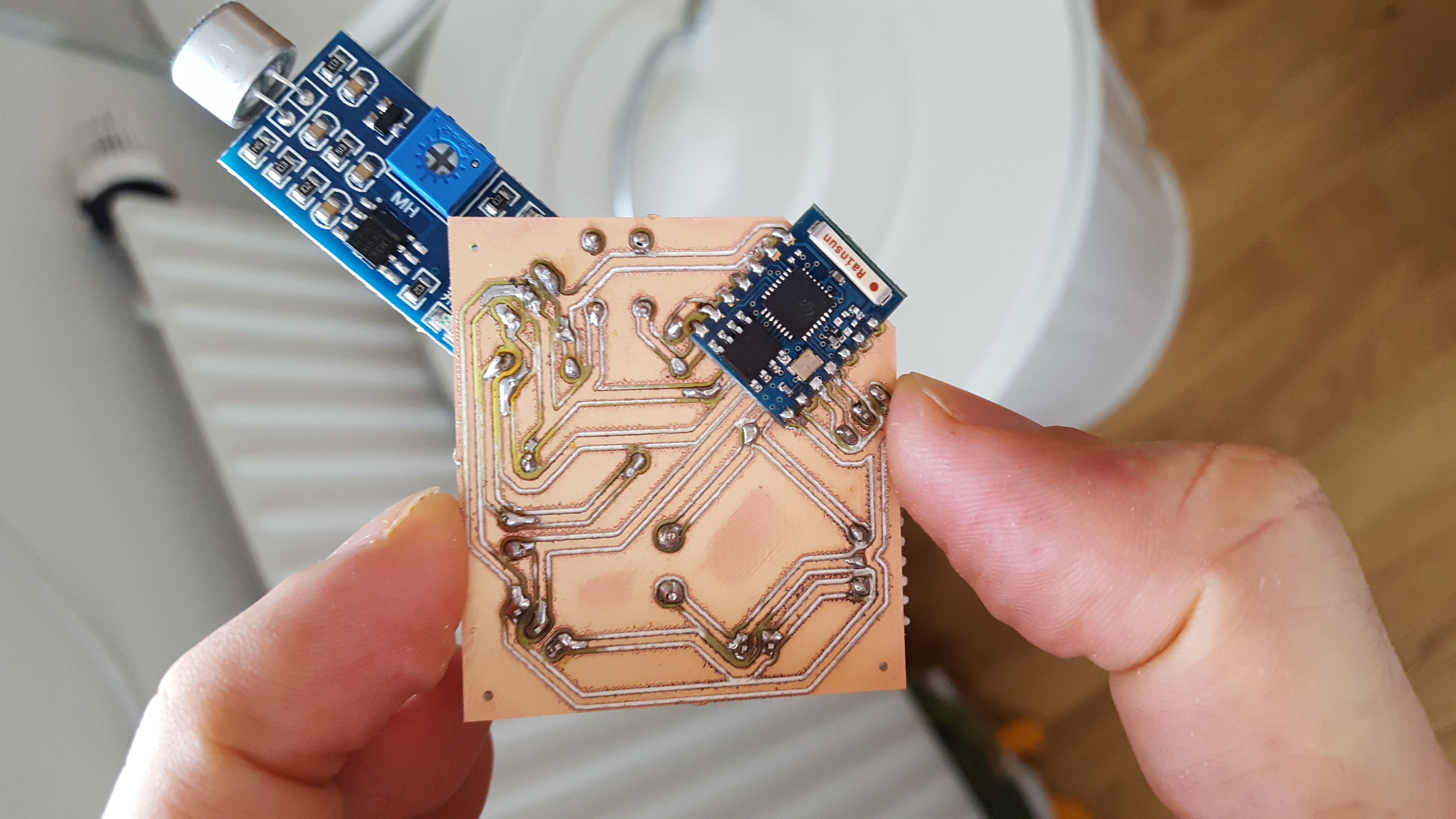
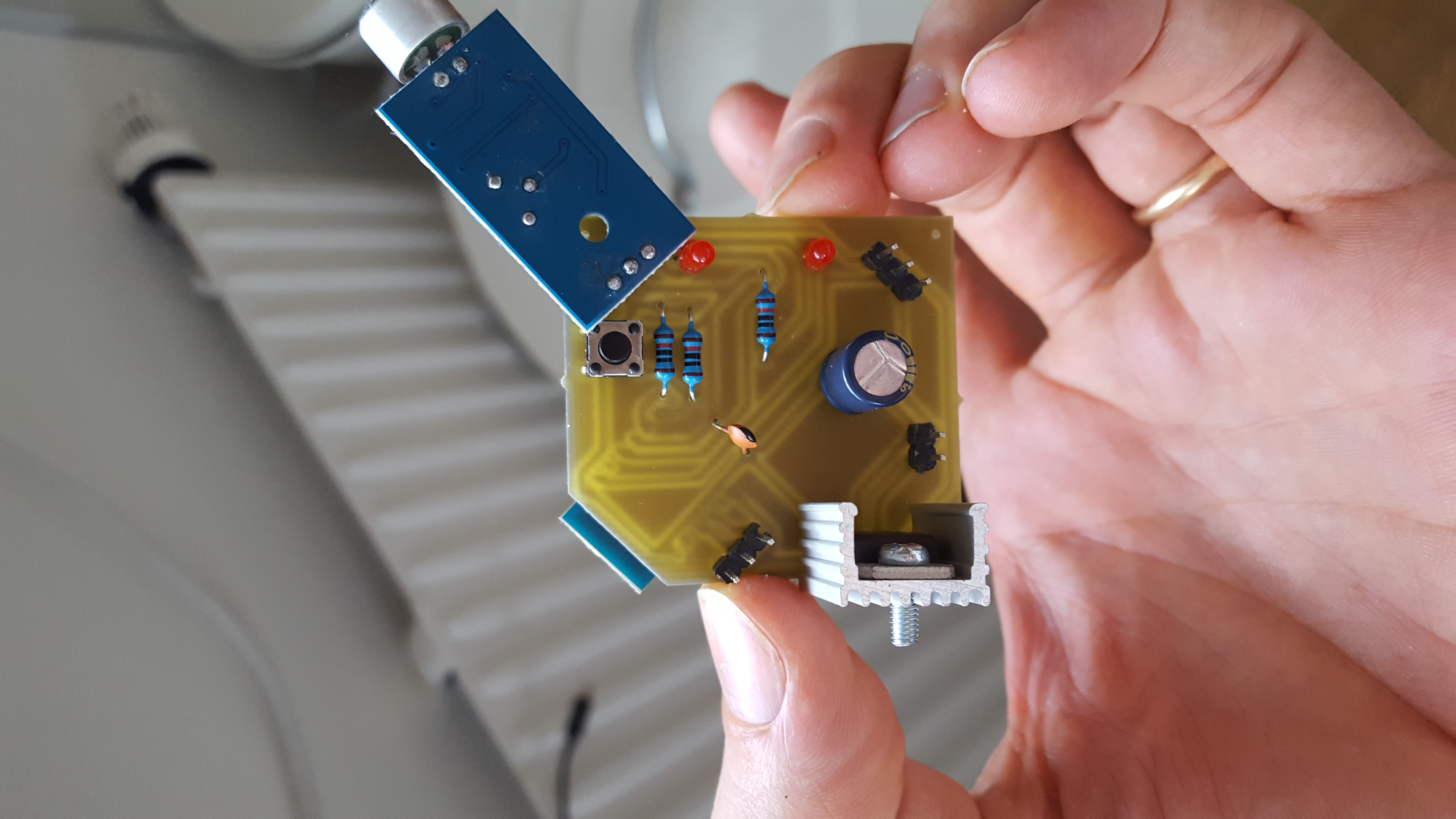
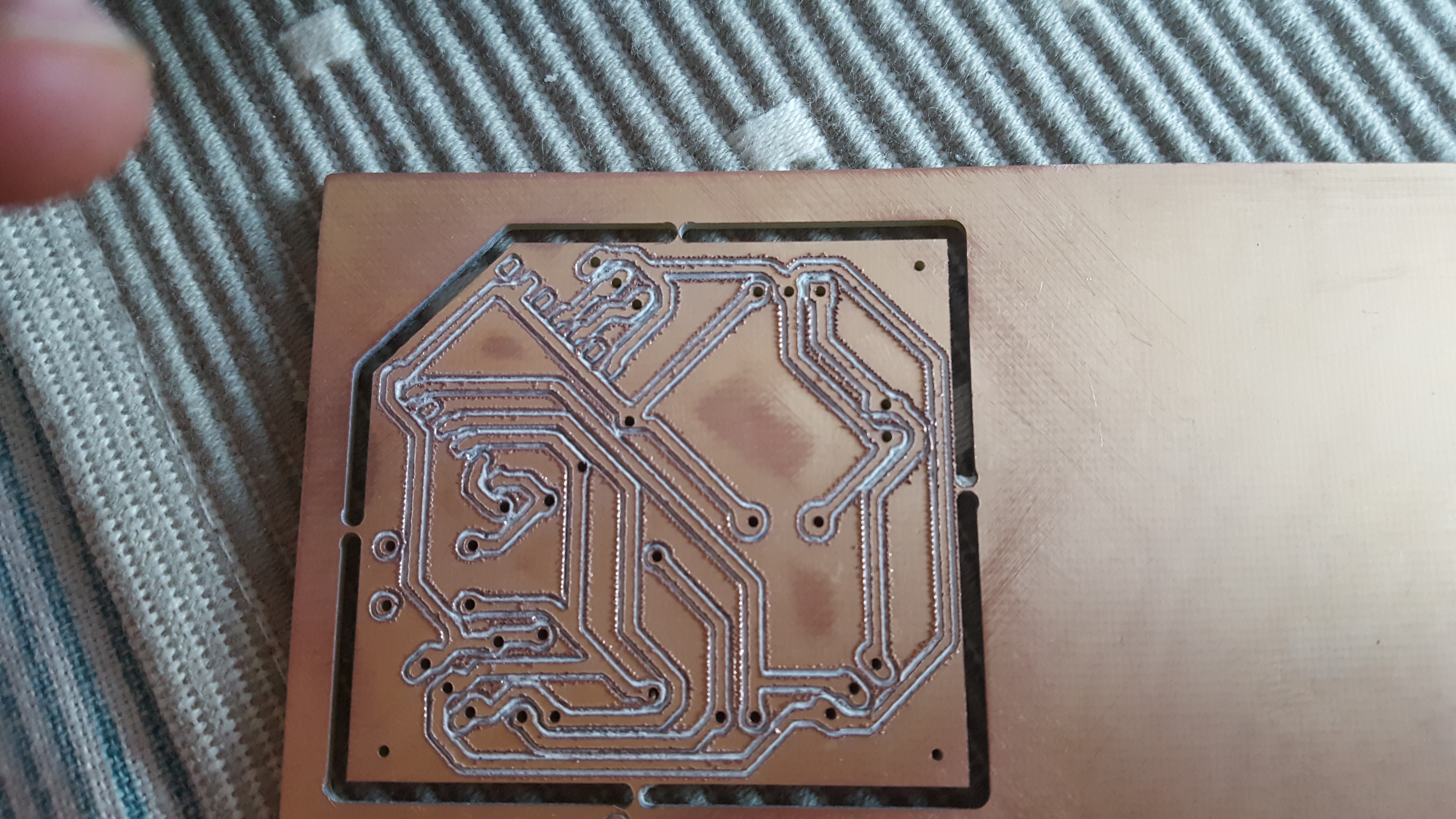
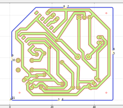
Here is my first milled PCB. This is my electronics project I moved aside when I started building my MPCNC. It only has a Pro Trinket and 3 devices so the hook up isn’t too complicated. But I need at least 5, maybe more of these. I haven’t found any PCB milling software with an easy learning curve, so I just made a 3D model, generated the G Code in Estlcam, then cut it.
It took 3 attempts. I milled a pocket in pink foam board, then put the circuit board in the pocket. I gave this 2 tries, but I wasn’t satisfied with it so my last try I made a pocket in MDF. The MDF worked best. It’s a 2 sided circuit board, so I did it in 5 cuts. Drill, engrave, pocket, (flip the board over) engrave, and pocket.
I tested it with an ohm meter, and it checked out. I will need to clean this up and cut it out next.
Dave


I didn’t try anything actually, but it seems that the best solution to make PCB is to use all the stuff from the Cyclone PCB Factory:
You can use GRBL for RAMPS (or at least GRBL for Cyclone: https://github.com/carlosgs/grblForCyclone ),
then you can use bCNC (free, autolevel, gerber files, milling, etc…) https://github.com/vlachoudis/bCNC
With GRBL for Ramps, you can still use Estlcam (and I think in a better way: you don’t need Repetier Host anymore and you can use autolevel, etc).
All the stuff of the Cyclone is as well documented as the MPCNC. Perfect for newbie.
I’m not an expert and I didn’t try all this stuff (still trying to find where is the 0.5mm slop I have on my MPCNC or trying to build a stronger CNC in mdf). But I don’t see any reason it won’t work with GRBL in your Ramps, it looks like better than Marlin if you don’t need to print in 3D.
Judging by the consistency of those lines, milling the pocket makes it extremely level. It looks great.
I tried to find software or some sort of PCB to test a while ago I gave up on the software after a few hours of screwing around and turned to SolidWorks for my little PCB test. I’ll need to find a guru to sit down with or maybe a good video walk through before I attempt that again.
Very cool. What size tools and depths of cut did you use?
I’m assuming you’re happy with your CAD solution, but if you really want to make anything more complicated, you are less likely to have wiring errors if you use a PCB CAD program. Something like eagle or KiCAD. In those programs, if your schematic is correct, then your layout has a high chance of being correct. The trick is finding a good part library, which had a 2D model of the part and a schematic. Sparkfun also has a big part library, which can really help getting started. Making parts from schematics is a pain, and most of the time, someone’s already done it. Doing this in 3D is going to be really tough when you start adding a lot more connections.
Sparkfun guide:
https://learn.sparkfun.com/tutorials/how-to-install-and-setup-eagle
The gist is:
- install eagle and get a good 1 or 2 parts libraries
- All all your parts to the schematic, including any pin headers (0.1" pin headers are useful if you actually solder on headers, or even just to solder on wires)
- Wire everything together in the schematic.
- Go layout, set the size of the board, move your parts around. Add holes for mounting, etc.
- Make your traces, adding vias to the other side of the board, if necessary, etc. You can adjust the size of the traces. You can also do an autolayout or autotrace if you are bold.
- Export it into a bunch of files… This is where it gets hazy, but the files are some standard format, with funny extensions, and they still need to be CAM’d.
I’m trying to remember, but when I did this last, eagle exported individual 2D files, something like a dxf for each layer, top and bottom, one for drill holes, and one for the perimeter, then I had to use something specifically designed for the PCB mill I was using to actually do that CAM.
Unfortunately, it is a steep learning curve, but if you’re already familiar with CAD, you’re going to be a step ahead. When you get your first PCB cut though, you will have learned 90% of the program. There’s no escaping that. You might also try to just find some eagle files out there to play around with. Again OSHPark has some shared designs:
https://oshpark.com/shared_projects
When you do learn a program like this, you can definitely whip up some boards pretty quickly, and when you are done, you can just inspect the schematic to see what was wired where. It’s a very useful debug tool. The schematics can also have little subsections to make them easier to understand. I’ve seen some very complicated PCBs made this way, and with very few errors and revisions.Then when it comes time to put them into service the schematics were the only way to find out where to debug things.
What size tools and depths of cut did you use?
I used all Dremel bits. To cut the traces, I used a 30 degree engraving bit. The pockets I found the smallest diameter bit I had so I’m not sure what it is. I think it’s a diamond bit, it looks like a gritty metal. It has a slight taper, flat on the bottom. This bit has a 2mm diameter at the bottom.
For engraving: 30 deg V, 5 m/s feed, .3 mm steps and a total depth of .6 mm.
For the pockets, I just needed to remove the coper: 2mm Dia, 5 m/s feed, .3 mm steps and depth of .4mm.
Most of my PC boards are one-off and include a micro-processor like an Arduino, so I make them with perf board, or 3D printed. If your interested, I have several examples here: http://www.instructables.com/id/Custom-Circuit-Boards/
I do a lot of prototyping before I solder, so I’m not to concerned about getting something wrong. I use Fritzing to document my wiring and I also use it to manually route the wiring for my one-off boards. I used Fritzing to do my wiring layout for this project, so I already knew about what it would look like before I made the model.
I will figure out a better software in time, I was just anxious to see if I could get the accuracy to do it. The MPCNC looks like it will do nicely.
I just tested my MPCNC for PCB-milling and it worked great!
The outcome needed some sanding but that’s because I need to get some better end-mills or V-bits and fine tune the speeds and widths…
I made a simple post processor to clean up the gcode form FlatCAM, you can find it and an explanation on how I did it on my github
/Kalle